


HOW TO DESIGN A PCB LAYOUT?
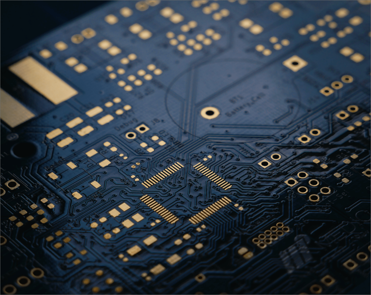
Printed circuit boards also known as PCB are plates made of various insulating materials with conductive tracks and islands on the surface for mounting electronic circuit elements and with solder-coated holes between the surfaces.
HOW TO DESIGN A PCB LAYOUT?
Printed circuit boards also known as PCB are plates made of various insulating materials with conductive tracks and islands on the surface for mounting electronic circuit elements and with solder-coated holes between the surfaces.
The board itself is an insulating and inelastic material. (There are also flexible PCBs) The thin connections seen on the surface of the board are Part of the conductive foil that covers the entire board at the beginning of the production phase. This conductive foil is partially etched and the remaining copper paths form a network. These paths are called the Conductor Pattern and provide the electrical connection between the electronic parts mounted on the PCB.
PCB has two important purposes;
- Keeping electronic components together,
- It is to provide electrical connection between components.
PCB design is one of the basic steps in the production of systems. Making a good PCB design will prevent problems that may arise during production as well as minimize the financial problems associated with it. There are rules and application methods to be considered during design.
PCB Design Equipment
There are many computer-aided design packages available for commercial development programs.
There are also very good packages available at a modest cost for those interested in PCB design as a hobby and even for students.
The software capacity of PCB programs varies considerably. More affordable and even free software provides basic functionality, while top-level packages allow much more features to be included in the design. There are simulations, complex routing and many more features in such programs.
Circuit Schematic Capture
The first phase in development of a PCB layout is to capture a schematic for the circuit. This may be achieved in a number of ways. Circuits may be entered into a capturing tool. This may form a part of design package or it may be an external package which output may be exported in a suitable format.
In addition to performing schematic capture, circuit simulations may be realized at this stage. Some packages may form a interface for the simulation packages. For applications such as RF circuit design of the circuit will enable the final circuit to be optimized more without forming an prototype
When the schematic capture is completed, the electronic design of the circuit takes place in the file and may be transformed into what is termed as “netlist”. The Network list is the interconnectivity information and it is essentially the component pins and the circuit nodes, or nets, to which each pin connects.
Initial PCB Component Placement
It is necessary to gather a rough idea about where the components may be found and if there is enough space for all the necessary circuits before moving on the detailed PCB design and layout. This will explain the required number of layers in the board and will enable decisions about whether there is sufficient space for all the circuits.
After making a rough guess about the circuit space and their approximate locations, a more detailed component design may be created for PCB layout. This can take into account issues such as proximity of the devices which may need to communicate with each other and other information related to RF.
In order to components to be included in PCB layout, they need to have all the information relevant to themselves. This information will include the area occupied by the printed circuit board pads, any kind of drilling, retention areas and more. Typically, several devices may share the same footprint, therefore there is no need to enter this information for every component number. However, a library will be built for all the devices used in PCB layout design system. In this way, all the components used previously may be easily called.
Routing
Once the basic placement is completed, the next step of PCB layout is to route all connections between all the components. PCB software then route physical connections on the board according to network listings in the schematic. In order to achieve this, it wil use the available number of layers for connections by creating holes as required. Often, a layer will be allocated to be used as a ground plane and another one as a power plane. Not only this reduce the noise level but also enables low source connections to be made for power.
Routing may use a considerable amount of computing power. This is especially valid for larger designs which may include more then three or four thousand components. When the routing is difficult because of high density of components, this may cause Routing take a significant amount of time.
PCB Files
The information for the photo graphics of PCB layout are output as Gerber files. This format is standard for PCB files and it is a numerical control file form which is used by a photo plotter. In addition to Gerber files, drill information is also generated along with screen print and photo-resist information.
One of the main elements in the cost of a printed circuit board is drilling. In any desing, some holes are required for fixing as well as the ones required for any conventinal components. However, to reduce the costs it will be wise to use as few holes as possible. This way, the drill will need changing less and more time will be saved.
Once complete, PCB information will be used in many areas of manufacturing process. The files may be used for developing a pick and place program and additionally may be used in manufacturing of PCB solder maks in order to add a solder paste to the board prior to component placement. The files also may be used to develop test programs such as “In-Circuit Test” (ICT) and specifically in development for any kind of nail bed test fixture.
In this way, PCB layout is a very important element of the whole manufacturing process for any product. PCB layout is more than a design for a basic board.
Refine is Lanner’s Authorized Distributor In
The Middle East, Türkiye And Pakistan.

 Call Us
 Be Reseller
